During my eighth semester at IIST, I worked on the design of an On-board computer as part of my project work. The OBC Board, also called the Command and Data Handling (C&DH) subsystem is designed to be used in small satellite projects.
The OBC Board is built around the SmartFusion 2 SoC FPGA which incorporates ARM Cortex M3, SRAM, SECDED, eNVM, RTC and various other features. This chip works at 3.3 IO supply and 1.2 V core supply. C&DH includes one SD card slot, one 64Mb SPI-Flash, one ADC and one 9-axis IMU. It uses TPS3813 for voltage supervision and as external watch dog. In-order to make the design isolated, Power and Signal Isolators have been used. One additional advantage of using isolators is that those pins for interface can be left unused without causing any risk to the system. The OBC board is a six layered PCB with the FG484 ball pin IC (M2S090). Figure below shows the Functional Block Diagram design of the OBC Board.
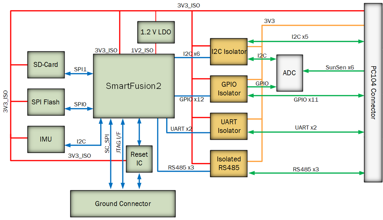
The OBC Board is compatible with the interface requirements for Ahan-1 and AAReST Mirror Satellite. Some additional interface (RS485 and GPIOs) are also provided for in-orbit testing and qualification experiment on the PSLV Stage-4 platform (PILOT). All the digital/ analog interfaces are connected to the small satellite PC104 standard connector. The number of interfaces provided is as follows -
- I2C - 6
- UART (3.3 V) - 2
- GPIO (OUT) - 7
- GPIO (IN) - 4
- RS485 - 3
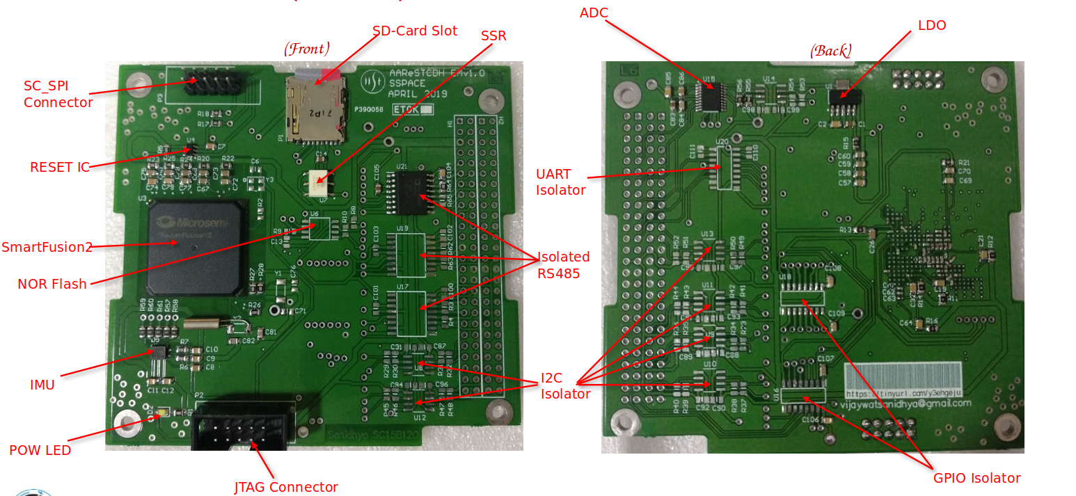
Salient Highlights of the board
Isolated Design
The Board contains various digital isolators for interface isolation with other sub-systems, if isolated power is provided then fully CDH design can be achieved.
In-Orbit Programming
System Controller SPI pins for programming have been provided so that in-orbit FPGA programming experiment can be conducted.
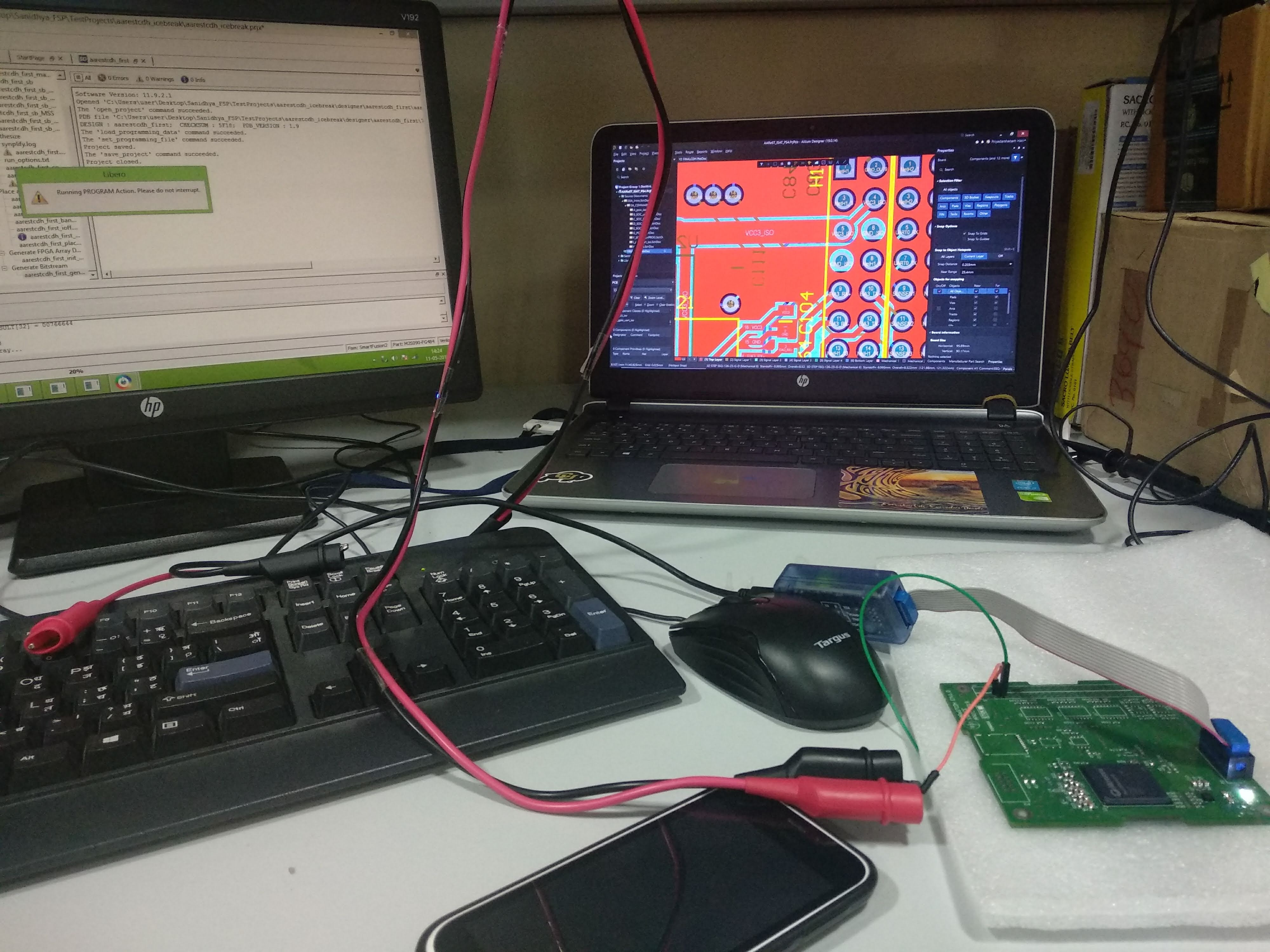
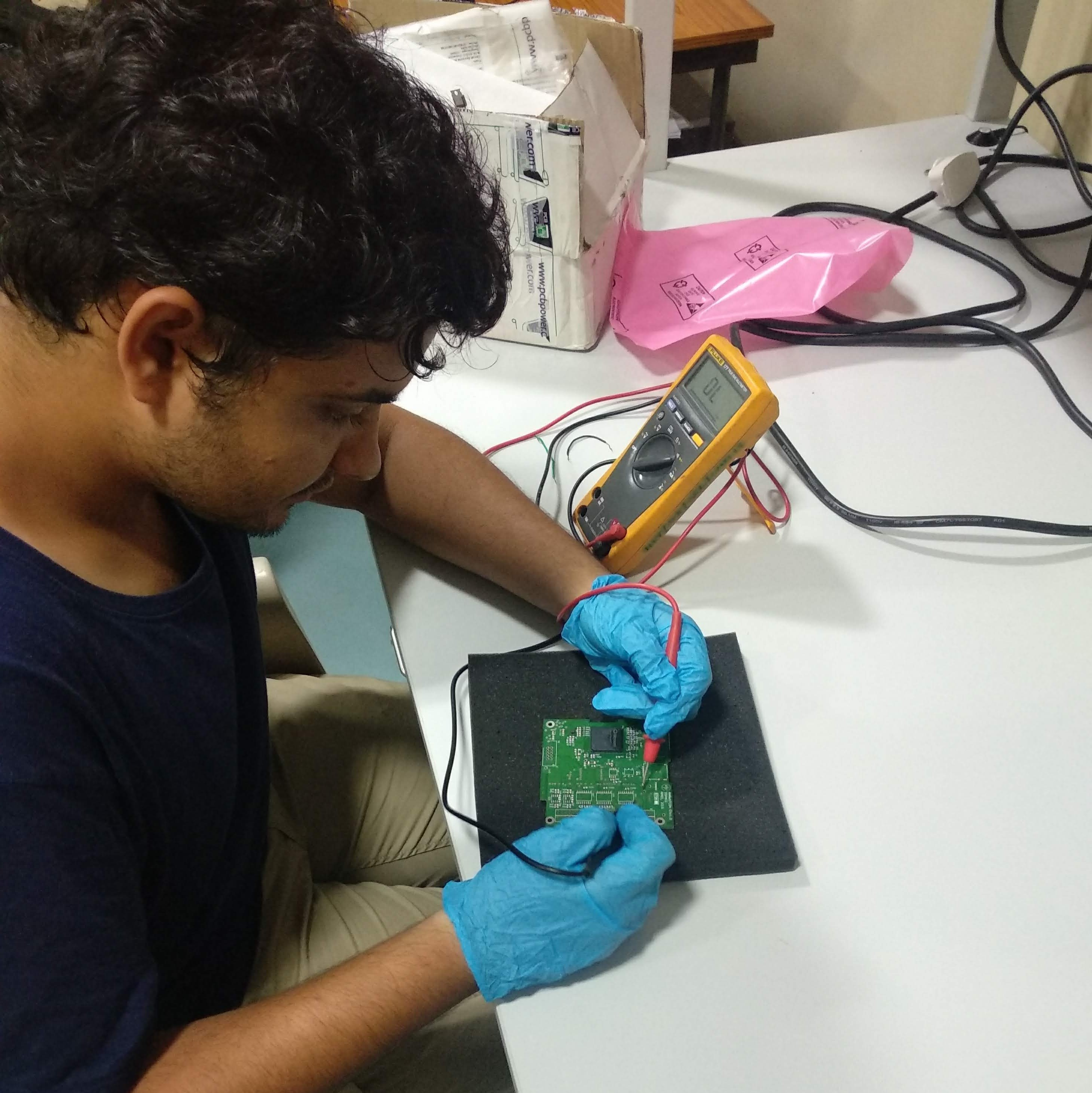
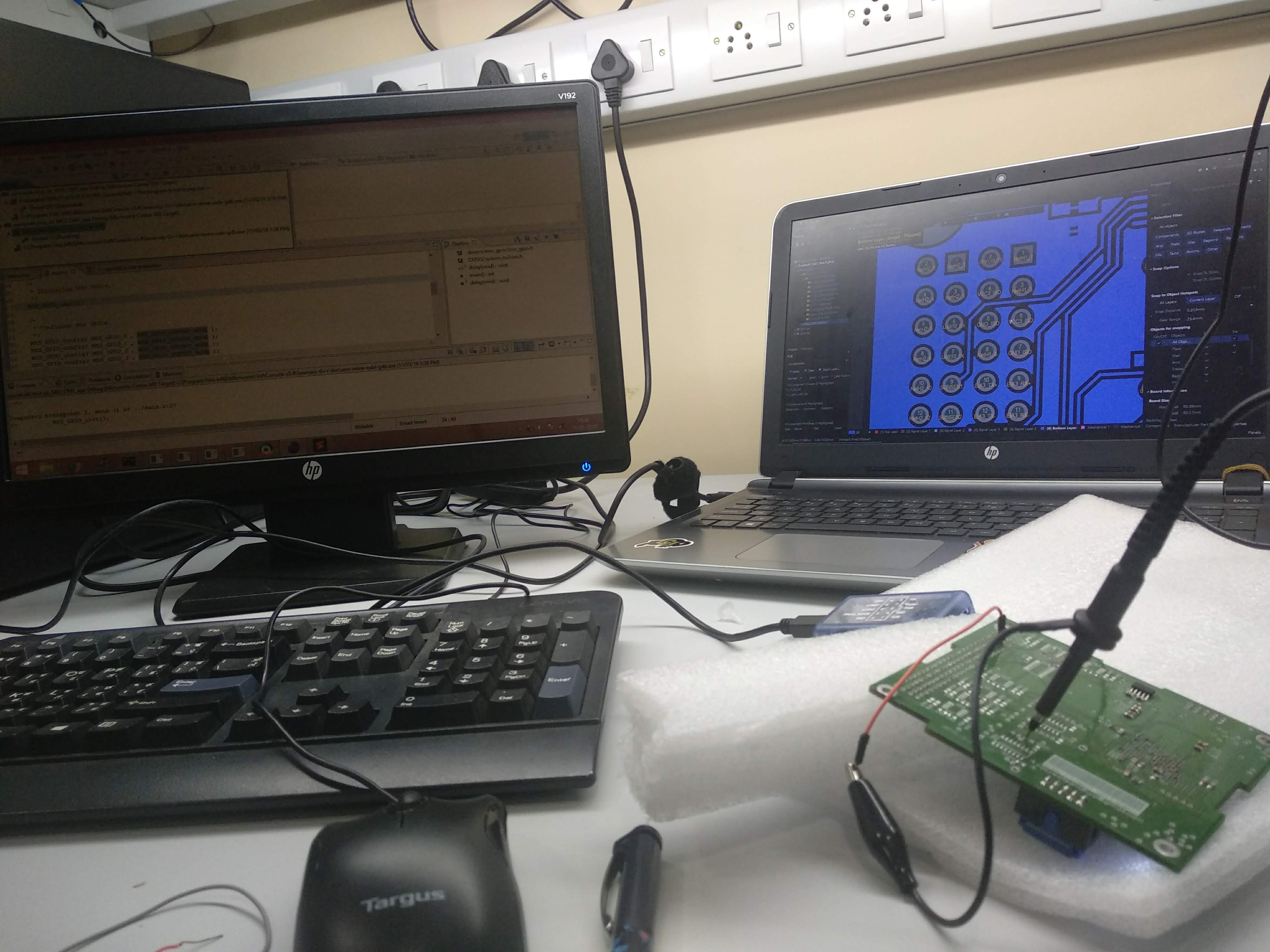
Here are some images taken during the testing of the OBC Board
